Evaluation Boards
Simplifying your future
GTJ Series
GAIA Converter has developed a series of test jig printed circuit boards (PCB) intended to ease GAIA’s product testing. The PCBs are for demonstration purpose only and are not intended for final application.
Parameters like isolation distance, copper thickness thermal management choices are not optimized for final application, but for test only.
The evaluation board service manual shows board schematic diagrams, layout, bill of materials, and outlines a simple process by which to populate the sample test jig.
In the manual, the expected performance of such jigs are given as examples.
EVGTJ2020

GTJ2020 empty test JIG rear view
Board dimension: 2.55″ x 4.3″ – 6,5 cm x 11 cm
Dedicated DC/DC architecture
Input range 9 – 60Vdc /100Vdc transient
2x8W or 2x20W
EVGTJ2020 is a test jig that can be used to evaluate converters from the MGDD08 or MGDD21 series, along with the LHUG150N input bus conditioner, and the FGDS6A100 EMI filter. Testing can be performed with regards to the MIL-STD-1275, MIL-STD-704 and MIL-STD-461 military standards.

GTJ2020 populated test JIG
EVGTJ2030

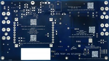
GTJ2030 empty test JIG rear view
Board dimension: 2.5″ x 5.9″ – 6,4 cm x 15 cm
Dedicated DC/DC architecture
Input range 9 – 60Vdc /100Vdc transient
40W or 80W
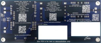
EVGTJ2030 is a test jig that can be used to evaluate converters from the MGDD40 or MGDD80 series, along with the LHUG150N input bus conditioner, and the FGDS12A100 EMI filter. Testing can be performed with regards to the MIL-STD-1275, MIL-STD-704 and MIL-STD-461 military standards.

GTJ2030 populated test JIG
EVGTJ2040

GTJ2040 empty test JIG rear view
Board dimension: 3.7″ x 7.3″ – 9,5 cm x 18,6 cm
Dedicated DC/DC architecture
Input range 9 – 42Vdc /100Vdc transient
160W
EVGTJ2040 is a test jig that can be used to evaluate a large range of converters from the quarter brick families of Gaïa-converter, along with filters, surge limiter and hold up modules. Testing can be performed with regards to the MIL-STD-461, MIL-STD-704, MIL-STD-1275, DO160 avionic and military standards. The EVGTJ2040 enables evaluation of global power architectures.

GTJ2040 populated test JIG
EVGTJ2050

GTJ2050 empty test JIG rear view
Board dimension: 2.75″ x 8.25″ – 7 cm x 21 cm
Dedicated DC/DC architecture
Input range 9 – 36Vdc /100Vdc transient
500W
EVGTJ2050 is a test jig that can be used to evaluate converters from the MGDM500 series, along with the FGDS35A100 EMI filter and LGDS600 Input Bus conditioner. Testing can be performed with regards to the MIL-STD-461 and DO160 military standards.

GTJ2050 populated test JIG
EVGTJ2060

GTJ2060 empty test JIG rear view
Board dimension: 4.3″ x 6.5″ – 10,9 cm x 16,5 cm
Dedicated AC/DC architecture
Input range 115Vac /400Hz
50W up to 3 outputs
EVGTJ2060 is a test jig that can be used to evaluate AC/DC converters from the HGMM35 or HGMM50 series, along with the MPGS14Eb Point of load.
Testing can be performed against Military standards MIL-STD-704, DO160, ABD100 and MIL-STD-461.
The board has also been designed in order to test separately up to 3 MPGS14EB with multiple sequencing modes.

GTJ2060 populated test JIG
EVGTJ2070

GTJ2070 empty test JIG rear view
Board dimension: 3.9″ x 7.1″ – 10 cm x 18 cm
Dedicated DC/DC architecture
Input range 9 – 42Vdc /100Vdc transient
200W battery charger
Compliant with following standards:
- DO160
- MIL-STD-704

GTJ2070 populated test JIG
EVGTJ2090

GTJ2090 empty test JIG rear view
Board dimension: 4.5″x 4.9″ 11,5 cm x 17,5 cm
Dedicated compact DC/DC architecture
Input range 9 – 60Vdc /100Vdc transient.
Up to 50W output.
Compliant with following standards:
- DO160
- MIL-STD-704
- MIL-STD-1275
- MIL-STD-461
EVGTJ2090 is a test jig that can be used to evaluate the FLHG60MN input bus conditioner in conjuction with the following DC/DC converter series : MGDD08N, MGDD21N or MGDD40N and MGDD80N.

GTJ2090 populated test JIG
EVGTJ3020-C

GTJ3020-C Architecture bloc diagram
Dedicated RailWay architecture
Input range 12Vdc to 160Vdc, 80W reinforced isolation, up to 3 double channels
EVGTJ3020-C is a test jig that can be used to evaluate the performances off DC/DC converters from MGRI or MGDDI series, along with the FLHGI-90 input bus conditioner.
GTJ3020-C contains 3 channels who can be tested separately with configuration straps.

GTJ3020-C populated with MGRI Series
Board dimension: 6.7″ x 6.3″ – 17.5 cm x 16 cm
